| Abstract:
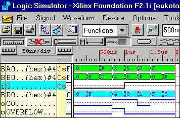
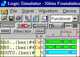
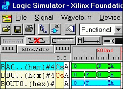
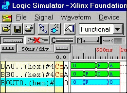
The Purpose of this lab was to use a multiplexor to combine several functions into one circuit, use a register to store our result value, and use a decoder to display the result in hexidecimal on the hex LEDs. |
| Procedure:
First, we tried to use tri-state buffers and they worked fine in the simulator but we could not get the design to compile so... we deleted all of the tri-state buffers and built a multiplexor. |
| Top Level (0) |
| Level 1 |
| Level 2 |
| Addition and Subtraction |
| And |
| Or |
| Xor |
| INPUTS:
A[0:3] (Pins 19, 20, 23, 24) B[0:3] (Pins 25, 26, 27, 28) Select[0:2] (Pins 77, 79, 80) CLOCK (Pin 56) C-In (Pin 78) |
| OUTPUTS:
HexDiplay[0:6] (Pins 49, 48, 47, 46, 45, 50, 51) Carry Out (Pin 61) Overflow (Pin 60) |
| Conclusion:
We learned a DAMN LOT from this lab! The lab itself was too big in my opinion. We learned how to use buses, lots of hierarchy, not to name our hierarchy the same as hierarchy in other libraries we're using (hehe), how to decode for the digital LED display, how to use the multimeter to trace pins to what they're locked to. |